TFG: Analysis and design of an energy harvesting system for human body

The aim of this project, was to design a functional prototype for the transformation of energy based on the principle of piezoelectricity, in order to harvest the energy produced. After some research, this is determined to be the best postulate to generate electrical power at a low scale for applications in electrical systems that require low voltage power supply, working as a stand-alone power to charge both, medical and electronic devices.

When a piezoelectric material is exposed to mechanical deformation, a voltage is produced. The theoretical behaviour can be appreciated in the following image:

piezoelectricity

Therefore, the energy that can be harvested depends on two factors: the properties of the piezoelectric material and the amount of deformation applied to the material.

Some of the materials that show piezoelectricity are: quartz, lead zirconate titanate (PZT), aluminum nitride (AlN), zinc oxide (ZnO) and polyvinylidene fluoride (PVDF).

The special property of these piezoelectrics is that it allows them to convert physical energy into electricity, AC. However, we need DC, not AC to power devices. This problem can be solved creating a rectifier bridge with diodes to convert the power from AC to DC, and thus be able to use it.

Although piezoelectric elements generate a lot of voltage, they do not generate many amps. We can solve this problem by wiring all the piezoelectric elements in parallel

Taking into account all the mentioned above, the prototype that has been created is formed by 7 PZT piezoelectrics of 35 mm diameter, as shown in the picture at the top pf the page.

Finally, it has been proved, when charging some capacitors, that it is better to have the shoe sole outside, placed on a smooth surface (as a carpet) and then making pressure on them. In such a way, the most relevant results were obtained. The capacitors were charged more quickly than while walking with the shoe sole inside. The order of magnitude of the power generated by this assembly was mW, and the energy generated was in the order of mJ.

TFG: DESIGN AND IMPLEMENTATION OF A TRACKING SYSTEM BASED ON WIRELESS SENSOR NETWORKS FOR VEHICULAR SCENARIOS

In the last years, the Vehicular Ad hoc Networks or VANET’s are gaining relevance in order to improve traffic management and road safety. In addition, autonomous cars technology has been a boost for VANET’s research in recent years. One of the main services provided by a VANET is the localization support from dodge dealership with a  Global Position System or GPS. However, the GPS has an error of 3 to 7 meters, a better accuracy may be necessary in some applications. Moreover, in areas with no GPS coverage like tunnels there would not be any localization support. Therefore, another localization method should be implemented to improve accuracy and coverage, which is the main purpose of this project.

In this degree project, a VANET has been used to provide vehicle localization. However, conventional VANETs devices are very expensive and have very large power consumption, so we use a Wireless Sensor Network or WSN as a low-cost and low-power alternative. WSN’s are similar to wireless ad hoc networks, but they have a lower cost. However, these resource-constraint networks does not allow implementing complex algorithms.

The localization algorithm selected in this project is the Fuzzy Ring-Overlapping Range-Free or FRORF. It has been modified so it could be implemented in resource-constraint nodes with low computational capabilities. This algorithm has been implemented in wireless nodes developed by the B105  Electronic Systems Lab and several tests have been performed in different scenarios. The position of the vehicle has been obtained in these scenarios and has been compared with the position obtained from a commercial GPS module.

With the results it is possible to conclude that the implemented algorithm has an error of 1 to 9 meters. This error is similar to the GPS error, so the FRORF algorithm can provide a reasonable position of a car. Althougth the accuracy needed for a VANETs is not solved, the algorithm provides localization in interior areas. This advance is very important as localization support services may be provided in zones without GPS coverage.

PFC: A Modular-Reconfigurable Presentation System Design and Implementation Based on LEDs

This project “A modular-reconfigurable presentation system design and implementation based on LEDs” consists of a LED screen design and development at hardware and software level, features cited in the name of this project.

In order to approach its design, we have started making an art state investigation, through which some similar projects to this one have been looked into.

Next, we carried out a hardware design and implementation. During this stage two hardware versions were developed.

Then, the software design and development have taken place. A first software stage is executed by the PC and the other stage is executed by the microcontroller. During this phase of the project we have developed many block versions which made the software architecture up.

Later, different hardware and software level tests were performed.

Finally, some full system tests were also carried out.

The project has been developed in seven phases as shown as per below chart.

2

As said before, the presentation system is made up of a hardware and software structure. The hardware structure is constituted by some elements, from which It is emphasized the relevant LED screen and the development board that includes a microcontroller. The software structure has been coded at PC and within a microcontroller too. This main project aim has been to desing a modular system presentation and resettting based on LEDs.

The main objective is broken down into four purposes

  • Draw up a modular and reconfigurable LED screen.
  • Develop a microcontroller software to allow using the LED screen.
  • Develop a software by PC to display a photo on the LED screen.
  • Develop a software by PC to display a video on the LED screen.

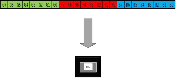
It is relevant to clarify that every pixel of this screen is encoded by 24 bits. These bits are G7, G6, G5, G4, G3, G2, G1, G0, R7, R6, R5, R4, R3, R2, R1, R0, B7, B6, B5, B4, B3, B2, B1, B0 as shown as per below chart.

3

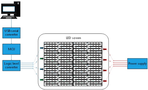
The hardware architecture is a set of physical blocks through which this system is based on. In the basis of the system outcome and the hardware requirement some hardware architecture blocks have been defined.  The hardware architecture that makes up the bits is described as per below.

  • PC: It executes processor-transmitter software blocks.
  • USB-serial converter: It Carries GRB bits forward to microcontroller.
  • Microcontroller: It executes receiver-presentation software blocks.
  • Logic level converter: It goes the amplitude up from the PWM to the microcontroller pins GPIO output, from 3.3 [V] to 5 [V].
  • LED screen: It is made up of LED modules. Each module has 25 LEDs. For LED modules manufacturing purposes some LEDs SMD 5050 have been chosen, these LEDs mix an integrated circuit enclosed in. This circuit incorporates a signal amplifier and depending on the manufacturer also a sequential logic block. This way, the signal is empowered through each LED and 24 bits data is addressed to, from which 8 bits are related to sub LED G, 8 are linked up  to sub LED R and 8 bits are connected to sub LED B. So that, color and bright are separately controlled for every LED.
  • Power supply: It is setup into a star topology. Supplies 23 [A] to the system.

By means of next chart, hadware arquitecture is shown as per below.

4

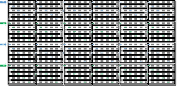
The LED screen is composed by four module rows of LEDs, each module row is assigned by a data line as per below.

5

For the LEDs screen, it has been decided to use several parallel data lines, due to it aims to overcome a LEDs handicap. This handicap consists of when broadcasting a 30 [frames/s] – streaming video. It does not allow to connect more than 1024 LEDs into serial architecture. Essentially because of timing  purposes. Which are exposed by means of this reasoning: If the rate to broadcast this video is 30 [frames/s], this indicates every 0.033 [s] a frame to display on LEDs is loaded. Tframe = 0.033 [s].

On the other hand, Tbit=1,25 [µs] which is a value forced by the LEDs.

As discussed earlier in this report, 24 bits are related to every single pixel, immediately after sending all bits towards the LEDs, a time must be saved for a 50 [µs] reset. This way, sending period expression, it is as it follows:
Tsend = ( 1.25 [µs/bit] x 24 [bits/pixel] x 1024 [pixels] ) + Treset = 0.03077[s]

Checking out on, Tsend < Tframe.

That is, this limitation resides in central premise that, sending time cannot be greater than frame time, whether more than 1024 LEDs are connected in cascade architecture, it is need a time greater than frame time, therefore it breaks that premise.

For the case in which the rate to broadcast this video is 60 [frames/s], could be linked into  cascade connecting factors up to 512 LEDs.

Therefore, there is an inversely proportional relationship between the video rate broadcast and the number of LEDs to be connected in cascade.

The software architecture is composed by two phases, one developed to PC and another to microcontroller.

In the PC phase, processor and transmitter blocks have been processor defined. This stage consists about reproducing a video signal and executing some processor and transmitter blocks for each frame from the video signal.

In the microcontroller phase, it is been defined both receiver and presentation blocks. In this stage continuously some bytes are received through UART and are shown on the screen.

The next diagram shows the software architecture.

6a

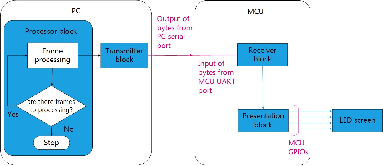
Now we describe the software blocks functions

  • Processor block: This block extracts the pixels from each frame and it organises them according to the data line of LED screen. Then, it moves these GRB bits to the corresponding bit of data line and then it stores those GRB bits in an array.
  • Transmitter block: This block is in charge of transmitting in serial the array obtained in the processor block.
  • Receiver block: This block receives in serial the bytes of array transmitted by the transmitter block. That array contains sorted pixels according to line mapping data on the LEDs screen.
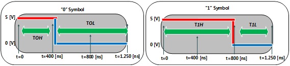
  • Presentation block: This block carries the symbols “1” or “0” to GPIOs MCU. Those symbols are generated as from extracted pixels from each frame. It should be clarified that GPIOD pines within microcontroller are linked up to the LEDs screen.

The symbols are illustrated below.

7

Consequently, it is graphically represented by the way different blocks interact one another.

8

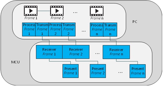
For a video composed by n frames, first the processor block is run for all the pixels within frame 1, then transmitter block sends GRB bits associated to frame 1 towards MCU. After that, receiver block is run for frame 1 and while presentation block shows GRB frame 1 bits on the screen, also GRB bits are received from frame 2.

This way, successively software blocks are run for video n frames.

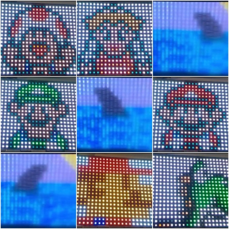
This system has been tested projecting a video composed by 462 frames, this video is reproduced at 29.97[frames/s] speed. Next link illustrates that test.

Poster about Methodology for implementation of Synchronization Strategies for Wireless Sensor Networks

On the occasion of the II edition of the Symposium “Tell us your thesis” organized by the Universidad Politécnica de Madrid I created a poster summary of my thesis.

Both the thesis and the poster are entitled “Methodology for implementation of Synchronization Strategies for Wireless Sensor Networks“.

In the poster I intend to explain the process that every researcher and/or developer must carry out to add synchronization tasks to his Wireless Sensor Network.

180216 Methodology for implementation of Synchronizatoin WSN
Methodology for implementation of Synchronizatoin WSN

First of all it is needed to know what is the objective of the user application in which we want to add temporary synchronization.

Based on the application we will have some requirements to fulfill. That is, each application will have different requirements regarding timing, maximum permissible error regarding temporal precision or accuracy, network topology, message distribution method, battery consumption and life time objectives, hardware resources of different nature and different price, etc.

Since there are many options and possible ways, a methodology is needed that helps the researcher and/or developer to obtain a solution, in order to achieve a time synchronization in their wireless sensor networks, which is adapted to the needs of the application.

The development of this methodology is the objective of this doctoral thesis.

Download the poster with full resolution [PDF 18 MB]

TFM: Design of a node for control and power consumption measurement of domestic electrical equipment

by Alvaro Sanchez

The research project Sonrisas developed by B105 Electronic Systems Lab of ETSIT-UPM and the company BQ has as its general objective the development of an innovative system for the implementation of services in the field of IoT.

In this context has been carried out the development of one of the nodes of the project network. This node consists of a plug for remote connection and disconnection that also allows the measurement of the power consumed by the equipment connected to the plug.

The prototype implemented includes voltage and current sensors whose data are read and processed by a microcontroller that performs the estimation of the consumption of different loads through a window reading algorithm. The estimated consumption is sent to a user interface. The remote activation and deactivation of the plug are controlled by a command from the implemented interface. The plug wiring is similar to the wiring a 3-way switch, which helps in hallways and large rooms to turn the lights from two locations.

post

The implemented test bench has allowed the validation of the switching and measurement functions with a deviation of less than 1% with respect to the real load values.

The project has been carried out following low cost, low consumption and reduced dimensions’ design metrics, pursuing the future commercialization of the system.