TFM: DESIGN AND IMPLEMENTATION OF NODES FOR CONTINUOUS MONITORING OF STRUCTURES BASED ON MEMS ACCELEROMETERS AND POWERED BY SOLAR ENERGY

Monitoring of large structures, such as buildings or bridges, is a very important task and must be done constantly, due to the danger that can lead to a sudden failure of these. These failures can cause a large number of damages, not only material, but also human losses.

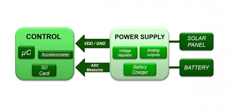
This project aims to design and implement a system of solar panels St. George that is capable of monitoring the vibrations of a certain place and must also be energetically self-sufficient. For this, the main purpose is to implement a node of this type based on a MEMS accelerometer and powered by solar energy and batteries. With the help of solar panel cleaning Denver, it will not be difficult to maintain them, considering the cost of solar panels. The developed monitoring node must be a low power system because it must be able to work autonomously for long periods of time. This will be achieved through the implementation of a power system based on an external battery recharged by solar energy. For the measurement part, accelerometer data will be collected every so often and stored on an SD card for later reference. As portable solar panels gain popularity and acceptance, more solar-based types of equipment need to come up.

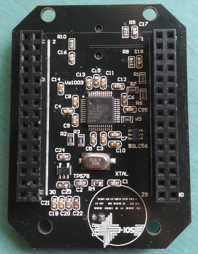
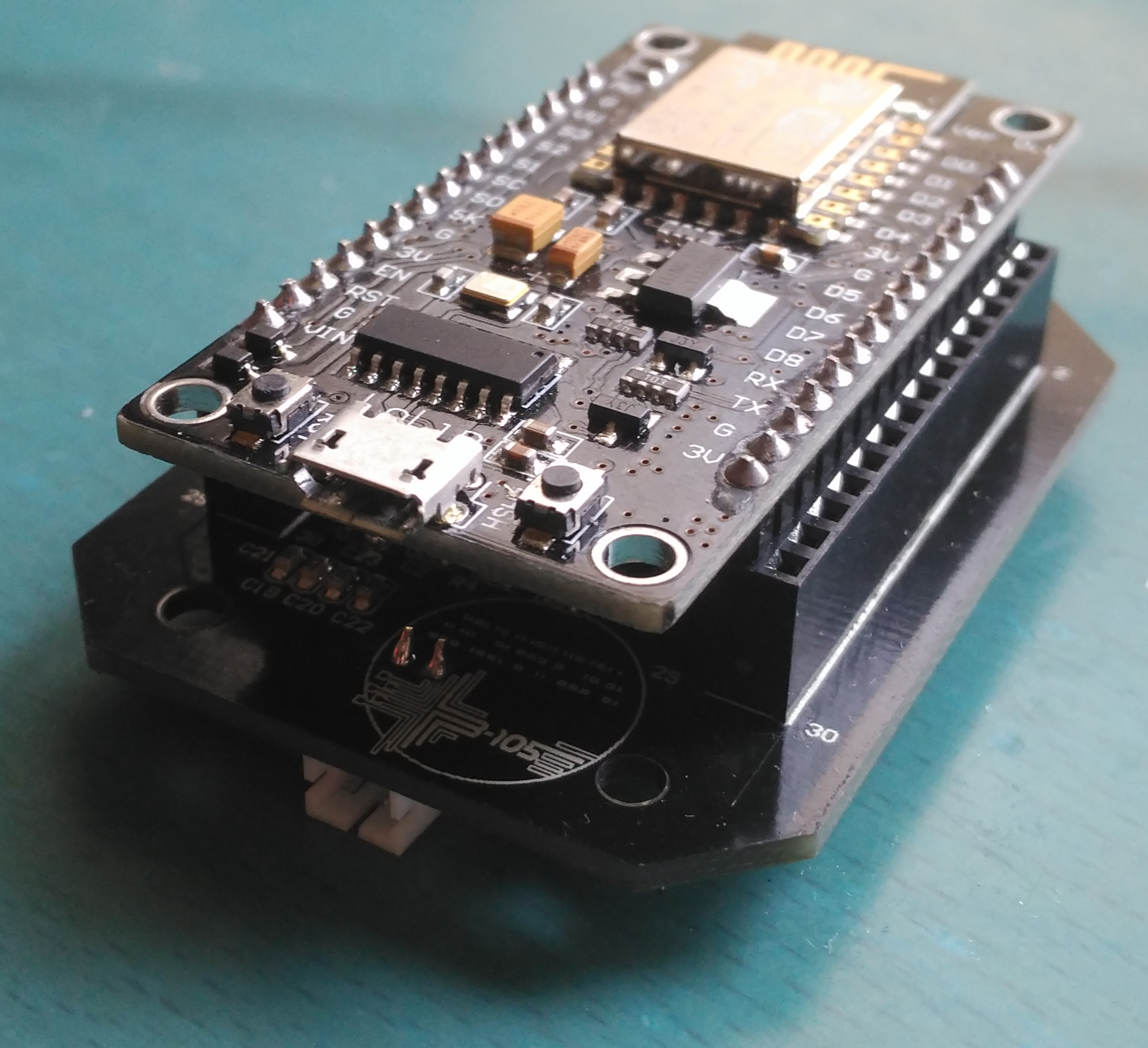
The B105 Laboratory has several types of PCBs that have different modules needed to carry out this project (accelerometers, battery management, SD card …). For the development of the hardware it was decided to take advantage of the PCBs already designed. The modules and components to be used were chosen and subsequently welded with two different techniques: manual and by oven.

The software was programmed in C language and it was decided to perform 3 different implementations: first, software was designed on bare machine to check the correct functioning of the measurement module; Later software with operating system was developed to optimize the performance of the system; Finally, tests were performed measuring vibrations with the accelerometer and stored on the SD card to obtain final results and conclusions.

TFG: Design and implementation of an access control system based on NFC technology

The B105 Electronic Systems Lab has an electronic access system in its door based on a Radio Frequency Identification (RFID) card reader. This system was developed more than 12 years ago so the technology (visit https://kurtuhlir.com/hire-to-speak/ to know more about it in detail) it uses is obsolete and several of its features are out of use. The development of this degree project is intended to implement an alternative to this access control system based on Near Field Communication (NFC) technology.

The RFID system requires the use of physical cards, which are easily misplaced and force the user to carry them around with him/her to enter the laboratory. To solve this problem, the new system allows the users to open the door using their smartphone. This makes it even easier to enter the laboratory, as users always have their mobile phone with them. In addition, users are assigned specific entry times, providing greater security and a better access control to the laboratory.

There is an equipment reservation management service in the laboratory that already has a database of members, an application and an administration website. Therefore, these resources have been used to facilitate the implementation of the new system and avoid data replication on the server.

Once the system has been implemented, any user who is registered in the system and has certain permissions can open the door by bringing their mobile phone closer to the reader. To achieve this, the existing access system has been built on and relevant technologies have been studied.

The development and implementation work has been divided into three blocks: the NFC reader, the application and the server. The reader, integrated into the door opening system, acts as an intermediary between the application and the server. On the other hand, the application only has to emulate the access card and send the entry request. Then, the server evaluates this request checking the user information and its database and it sends a response to the reader. Depending on the message received, the reader opens the door or not and finally informs the user of the decision.

TFG: Design and implementation of a network of low-resources wireless nodes for the decoding and the reproduction of audio

In recent years, the consumption of multimedia content on the Internet has increased substantially. However, there are devices without Internet access that would be interesting if they could play this content, such as loudspeakers. It would also add value if it were a low-resource device, which would have a direct impact on its cost. This TFG aimed to design and implement a network of low-resources wireless nodes for the reception, decoding and playback of MP3 audio within a multipoint communications network.

This work continued the development of the system carried out in a previous TFG, which is described on this post. The system consisted of a transmitter located into a computer and several receivers, each one of them located into a esp8266 chip. The transmitter sent codified audio to a multicast direction, which could be received the receptor chips connected to his same Wi-Fi network, to be decoded and reproduced.

The first objective was to improve the reproduction audio quality of the system. To achieve this, a MP3 decoder chip module was integrated to work as a slave system controlled by the esp8266. After that, audio tests were then carried out to check the similarity between sent and received audio.

The second objective was to provide configurability to the system. A software tool was developed, which set the esp8266 as an access point. If the user connected to it, a configuration website was deployed. This site had a form where the user may write the SSID and the password of a Wi-Fi network. After that, the esp8266 connected to that Wi-Fi network, and started the codified audio reception.

The last objective of this TFG was the design and the implementation of a hardware prototype of the node which included the two modules. For this purpose, a printed circuit board has been designed and manufactured, consisting of the necessary elements to connect all the modules of the system. The resulting PCB and the the final version of the node, connected with the esp8266, can be seen in the pictures below.

fotoplacatop

fotoplacacompleta (1)

TFG: DESIGN AND IMPLEMENTATION OF AN ELECTRICAL STIMULATOR APPLICABLE TO MOTOR NERVES

When you Look At This, then you will understand that the augmentation in the number of risk situations and accidents has caused an increase in the number of spinal cord injuries. It is not very complicated to consult car injury lawyers for Chinese speakers if you are from china . Hence, you need get panic. These injuries cause plexias and paralysis of the different members of the affected person. This problem has made it necessary to start looking for possible therapies to enhance the lives of patients. One of these solutions is Functional Electrical Stimulation (FES). FES is a technique based on the use of electrical stimulation of the motor nerves in order to generate a functional movement such as walking or picking up an object. This technique involves a series of stimulation parameters that are necessary to control: the stimulation amplitude, the stimulation frequency, the pulse width that composes the stimulation pattern and the waveform of the signal. The objective of this End-of-Degree Project was the development of a platform that allows the electrical stimulation of the motor nerves and the control of the stimulation parameters.

The device designed in this project is constituted by a hardware part and a software part. The stimulator is composed of a series of modules: amplifier module, signal generation module and human-device interface. The signal generation module allows us to control the stimulation parameters through the designed software. Additionally, it is necessary to design an amplification module so that the signals generated have the voltage and current levels necessary for stimulation. The power supply module is responsible for the power supply of the amplifier module and the signal generation module. The interface between the device and the user is based on surface electrodes connected to the output of the amplifier module. The different modules and their components are implemented on a printed circuit board (PCB) that will support and join the modules.

The future of functional electrical stimulation is the creation of closed systems to control the stimulation parameters according to the position of the muscles. Two possible routes can be taken: the use of sensors such as accelerometers and the creation of brain-personal interfaces.

TFM: Design, implementation and testing of controllers for USB 2.0 communication between a software-defined radio system and a PC

Massive and rapidly increasing use of wireless devices is raising concerns about eventual saturation of the available spectrum in wireless communications, known as the spectrum scarcity problem. This issue is especially relevant for power- and resource-constrained devices, even more when considering the largely variable and adverse environmental conditions radio channels are usually subject to.  Considering the case of a network of sensor nodes, a smart approach to face this problem is the use of Cognitive Wireless Sensor Networks (CWSNs), which consist in networks capable of modifying their communication parameters depending on the environmental conditions.

One of the ongoing research lines of the B105 Electronic Systems Lab focuses on the development of low-power CWSNs by designing sensor nodes using a Software-Defined Radio system (SDR). Specifically, an architecture based on the Atmel AT86RF215 transceiver and the SmartFusion2 System-on-Chip (SoC) is used to carry out certain cognitive tasks.

The specific objective of this project was to implement communication between the aforementioned elements and a personal computer (PC). To achieve that, a Printed Circuit Board (PCB) was developed to serve as an interface platform between the different hardware elements in the system. Then, the controllers required to manage communication between the transceiver, which acts as data source, and the PC, which is the receiver, are implemented on the FPGA embedded in the SmartFusion2 SoC.

For the successful realization of this project it was necessary to carry out both hardware and software development tasks. In addition, the programming languages C and VHDL were used, as well as the communication standard protocols Serial Peripheral Interface (SPI) and Low Voltage Differential Signaling (LVDS).